
Harvesting electricity from thin air
- Aarvnd Jay
- Sep 30, 2023
- 2 min read

Sony Semiconductor Solutions (SSS) has developed a device that leverages stray electromagnetic (EM) waves present in the environment to generate power for Internet of Things (IoT) devices. This innovative technology enables the harvesting of ambient EM waves, which are already present in our surroundings, and converts them into usable electrical energy.
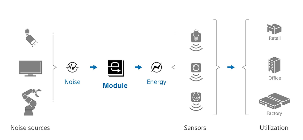
The device created by SSS utilizes cutting-edge energy harvesting techniques to capture and convert stray EM waves into a power source for IoT devices. These stray EM waves are generated by various sources such as electronic equipment, wireless communications, and other electromagnetic emissions that naturally occur in our environment.
By harnessing these ambient EM waves, the device can generate electrical power without the need for traditional power sources like batteries or wired connections. This has significant implications for the deployment and operation of IoT devices, as it eliminates the reliance on external power supplies and enables greater flexibility and scalability in their implementation.
The technology developed by SSS includes specialized components and circuitry that efficiently capture and convert the stray EM waves into usable electrical energy. The device incorporates antennas or other sensitive components that act as receivers to capture the ambient EM waves. These captured waves are then processed and converted into electrical power through advanced rectifier circuits or similar energy conversion mechanisms.
The converted electrical energy can be utilized to power low-power IoT sensors, communication modules, or other IoT devices. This eliminates the need for frequent battery replacements or the dependence on wired power connections, resulting in increased convenience, cost savings, and environmental sustainability.
The device's ability to harvest ambient EM waves opens up a wide range of possibilities for its application in various scenarios. It can be deployed in environments such as factories, offices, retail stores, homes, or any other location where electronic devices and wireless communications are present. The device can scavenge and convert the stray EM waves generated by these devices into a stable power supply for IoT devices, ensuring their continuous operation and reducing the need for external power sources.
Additionally, the device's energy harvesting capabilities enable it to provide insights into the status and performance of electronic devices. By monitoring changes in the harvested voltage or power levels, it can detect abnormalities or predict potential failures in the devices it interacts with. This feature is particularly useful in scenarios where device health monitoring, preventive maintenance, or fault detection is critical, such as in robotics or industrial automation.
Sony Semiconductor Solutions aims to collaborate with partners across various industries to develop and integrate this innovative energy harvesting technology into IoT devices and systems. By utilizing ambient EM waves as a power source, the company contributes to the advancement of sustainable IoT solutions, reducing reliance on conventional power sources and promoting environmental responsibility.


Comments